Matthew A. Stott1, Thomas A. Wall1, Damla Ozcelik2, Joshua W. Parks2, Gopikrishnan G. Meena2, Erik Hamilton1, Roger Chu1, Holger Schmidt2 and Aaron R. Hawkins1
1Department of Electrical and Computer Engineering, Brigham Young University, 459 Clyde Building, Provo, Utah 84602 2School of Engineering, University of California, Santa Cruz. 1156 High Street, Santa Cruz, California 95064 hawkins@ee.byu.edu
Abstract: Silicate spin-on-glass is used to coat PECVD SiO2 waveguides in order to smooth out surface topology and act as a moisture barrier. The measured optical throughput improved compared to uncoated waveguides.
OCIS codes: (130.3130) Integrated optics materials; (220.4000) Microstructure fabrication
Introduction
Silicon dioxide is an attractive waveguide material in the visible range because of its low absorption and low photoluminescence. Integrated optical devices meant for biosensing often incorporate SiO2 waveguides because efficient fluorescent molecules emit in the visible regime. Typical methods for depositing SiO2 films (chemical vapor deposition and sputtering) result in layers that have some degree of porosity [1] and water molecules tend to fill these pores causing an increase in refractive index with total moisture uptake. Any changes in refractive index can weaken intended mode confinement in SiO2 ridge waveguides. Films deposited over raised features can also leave unintended crevices and breaks that lower optical transmission. We have investigated using an overcoat of silicate spin-on-glass (SOG) as a way to address both of these problems.
2. Measurement of Water Uptake in PECVD Oxide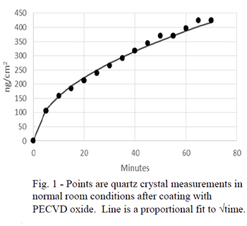
To demonstrate how atmospheric moisture can accumulate in thin SiO2 layers, an experiment was performed using a quartz crystal monitor typically used to measure deposition growth in a vapor deposition system. A 2µm PECVD oxide film was grown over the crystal (Maxtek) at a temperature of 250°C. The crystal was then placed into a monitor in normal room conditions. As can be seen from Fig. 1, which graphs the increase in mass per area for the crystal over time, the trend in added mass matches a diffusion profile (time). This trend strongly suggests that water molecules are indeed diffusing into the oxide and accumulating in the pores.
3. Spin-on-Glasses versus Deposited SiO2
In contrast to PECVD-deposited SiO2, SOGs are known to have better resistance to water diffusion [2]. There are two main types of SOG
Fig. 1 – Points are quartz crystal measurements in normal room conditions after coating with PECVD oxide. Line is a proportional fit to time.
material – silicates (which solidify into pure SiO2 matrices) and siloxanes (contains organosilicon compounds). Both generally have low initial refractive indexes ranging from 1.39 to 1.44. Here we consider silicate SOG layers, which are resistant to most wet-etch processes. Silicates have been considered for optical systems for many years, but their use has been somewhat limited by their maximum achievable thicknesses with good planarization, which tend to be around 500nm [3].
To demonstrate the differences between PECVD and silicate thin films, direct changes to refractive index were also monitored after these films were placed in water baths. The PECVD film measured was 5 m thick and grown at 250°C and the silicate (Desert Silicon P-640) was spun and cured to a 180 nm thickness. Both films were placed in 85°C water for about two weeks and their refractive index was measured using a reflectometer (thick film) and spectroscopic ellipsometer (thin film). The PECVD oxide’s index increased by 1.8% after the water bath while the silicate’s index increased by 0.3%, indicating a significant resistance to water diffusion by the thinner silicate film.
4. SOG Layer Improves Optical Throughput
To test the effects of silicate SOG on waveguide structures, a hybrid optofluidic device [4] was constructed that used PECVD SiO2 waveguides topped with thin (~500 nm, refractive index = 1.42) silicate protection layers. The optical throughput of this hybrid device was compared to one which only used PECVD SiO2 layers. Device design and fabrication are described in detail elsewhere [5], but they contained both hollow and ridge anti-resonant reflecting optical waveguides (ARROWs). This particular structure was used because the intersection between hollow and ridge waveguides is a challenging topology that creates a crevice break between the waveguides [6] – a break the SOG was intended to fill. A total of 6 µm of PECVD SiO2 (refractive index = 1.46) was used as the primary waveguiding layer in both device types.
After being exposed to atmospheric moisture for several days the optical throughput of the waveguides was tested using a 633 nm laser coupled into optical fiber and then aligned to various chips. Ridge waveguides approximately 4 mm in length were tested (five from an uncoated sample and six from a SOG coated sample) and the SOG coated waveguides showed an average increase in optical throughput of 28%. Waveguide structures which included the crossing of a liquid core chip were also tested from chip edge to chip edge (8 mm) as shown in Fig. 2a. With six devices tested for each design type, the throughput of the SOG covered devices improved an average of 47%. Fig. 2b shows an example of the optical mode output on the far side of the waveguide.
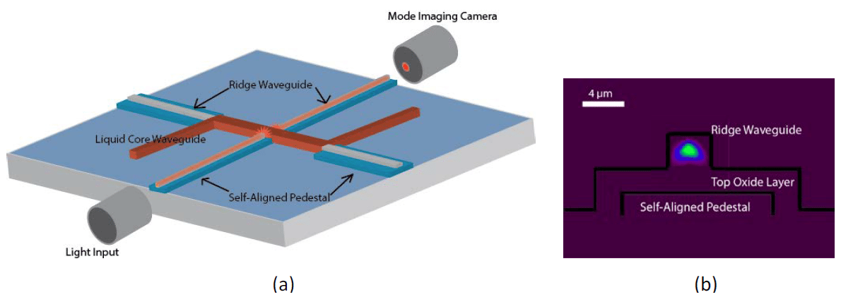
Fig. 2 – (a) Diagram of optofluidic chip used for testing properties of PECVD SiO2 waveguides with and without silicate SOG protection layers; (b) Output mode image for waveguide with SOG top layer.
In summary, we have presented using a silicate SOG as an overcoat layer for SiO2 ridge waveguides. Optical throughput was shown to increase for these hybrid structures. This improvement is likely due to the creation of a water diffusion barrier over the SiO2 surface or through filling up crevices created in the film deposition process. Further experiments are being conducted to isolate and quantify the positive effects of SOG.
Acknowledgments
This work was supported by the NIH/NIAID and NSF under grants 4R33AI100229, CBET-1159423, CBET- 1159453, CBET-1402848, and CBET-1402880 as well as the W.M. Keck Center for Nanoscale Optofluidics at the University of California at Santa Cruz. J.W.P. acknowledges support by the Eugene Cota-Robles Fellowship and the National Science Foundation Graduate Research Fellowship Program under grant DGE 0809125.
References
E. G. Parada, P. González, J. Pou, J. Serra, D. Fernández, B. León, and M. Pérez-Amor, J. Vac. Sci. Technol. A 14. 436 (1996)
N. Lifshitz and G. Smolinsky, IEEE Electron Device Lett. Vol. 12, 140 (1991)
R. Osredkar, Informacije MIDEM 31, 102, (2001).
H. Schmidt, and A.R. Hawkins, Microfluidics and Nanofluidics 4, 3 (2007)
E. J. Lunt, B. Wu, J.M. Keeley, P. Measor, H. Schmidt, A. R. Hawkins, IEEE Phot. Tech. Lett. 22, 1147 (2010)
Y. Zhao, K. D. Leake, P. Measor, M. H. Jenkins, J. Keeley, H. Schmidt, and A. R. Hawkins, Photonics Technology Letters 24, 46 (2012)